Cascade lasers are the newest generation of semiconductor lasers, currently only on the brink of commercialization. The Institute of Electron Technology in Warsaw has developed technology to produce mid-infrared GaAs based cascade lasers with a three times stronger pulse than previous lasers. The new devices pave the way for promising industrial and medical applications.
The Institute of Electron Technology (ITE) in Warsaw has developed technology to produce quantum cascade lasers of record-breaking power and built their prototypes. The new devices, made of aluminium-doped gallium arsenide, emit pulses of infrared radiation. In room temperature, the power of the pulse can reach up to several dozen milliwatts, and under cryogenic cooling . even five watts. These results are three times higher than those previously achieved for this material composition and design.
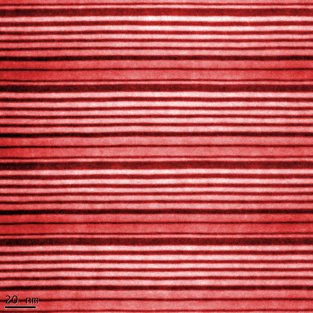
Quantum cascade lasers (QCL) are periodic structures made up of many (even up to several hundred) semiconductor layers, forming the so-called superlattice. The thickness of superlattice layers changes according to a careful pattern and usually amounts to a few nanometres. At the Institute of Electron Technology, layers are made of aluminium-doped gallium arsenide (GaAs/AlGaAs). They are deposited by means of molecular beam epitaxy.
QCL lasers rely on the mechanisms of conduction in semiconductor materials in a unique way.
According to band theory of conduction, low-energy electrons in a semiconductor, whose energy levels lie within the basic (valence) band, are bound to semiconductor atoms. If the energy levels reach those from the conduction band, the electrons break away from the atoms and become, along with holes, charge carriers in the material.
Traditional semiconductor lasers rely on the recombination of electrons from the conduction band in a semiconductor and empty, vacant states in the valence band to emit light. Hence, the wavelength of the radiation emitted by a semiconductor laser depends on the size of a band gap between the valence and conduction bands.
"It is not easy to build a semiconductor laser which emits radiation of a specific wavelength," says Prof. Maciej Bugajski from ITE. "First, we need to find a material with an appropriate band gap. This could prove a difficult, even impossible, task. And when we do have one, it is still only the beginning of the way, because we usually have to devise the processing technology from scratch".
In quantum cascade lasers, the energy of the emitted radiation to less extend depends on the material but rather on the geometry of the superlattice . that is on the composition and thickness of periodic semiconductor layers. An electron injected into the first period of the supelattice tunnels to a high region of the conduction band. A moment later the electron jumps to a lower level, still within the conduction band (intersubband transition). Photon emission occurs during the jump. Then the electron tunnels to a high region of the conduction band of the next period of the superlattice and the process repeats. The gap between the excited and basic state within the conduction band can be altered, for example by changing the thickness of superlattice layers.
The characteristics of QCL lasers make it relatively easy to design a semiconductor structure which emits electromagnetic waves of a specific wavelength. Cascade lasers built at ITE can operate in the mid-infrared region of the electromagnetic spectrum (waves up to 9-10 microns in length). "The mid-infrared is a highly attractive region of electromagnetic waves. This stems from the fact that many chemical compounds absorb radiation precisely from this region," says Prof. Bugajski.
The first QCL lasers in Poland were built in 2009 precisely at the Institute of Electron Technology. They were developed as part of the all-Polish .Advanced technologies for infrared semiconductor optoelectronics. project, coordinated by ITE. One of the participants in the project was the Institute of Optoelectronics of the Military University of Technology, where a prototype of an ammonia gas detector was built. Today, equipped with new cascade lasers from ITE and infrared detectors by VIGO System S.A., built in collaboration with ITE, the device can detect ammonia in concentrations of several dozen particles per billion.
Quantum cascade lasers have only been known for a few years. They are an object of great interest, as they allow to build portable detectors able to detect trace amounts of chemical substances, for example methane in mines or dangerous gases in chemical industry. Medical applications are equally promising. QCL laser in detectors could help detect even trace amounts of disease markers in the air exhaled by the patient. Given that infrared radiation passes through the human body, the lasers open up the possibility of safer medical examinations in a better resolution than that achieved in ultrasonography.
The Institute of Electron Technology in Warsaw (ITE) carries out research in the field of electronics and solid-state physics. It develops, implements and popularizes state-of-the-art micro- and nanotechnologies in photonics and micro- and nanoelectronics. The Institute focuses on optoelectronic detectors and radiation sources, state-of-the-art semiconductor lasers, micro- and nanoprobes, nuclear radiation detectors, microsystems and sensors for interdisciplinary applications, as well as application-specific integrated circuits ASIC. In order to allow easier access to the technology, construction and measurement services for industrial and science and research units, the Institute has established the Centre of Nanophotonics, the Centre of Nanosystems and Microelectronic Technologies and the Laboratory for Multilayer and Ceramic Technologies.
Back |
PDF English |
Polska wersja |
PDF Polski