The purpose of research and development work carried out at the Department is the structural, optical, electrical and photoelectrical characterization of materials and structures. Main methods:
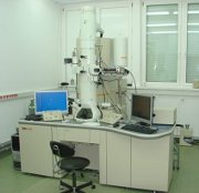
TEM - transmission electron microscopy (including HRTEM - high resolution, and STEM analytical techniques of TEM), FIB - focused ion beam system, and SEM - scanning electron microscopy.
The FIB system is used for the TEM-samples preparation, and also for many processes of micro- and nano-technology: deposition of metals (Pt, W) and dielectrics, as well as milling/etching of materials (including accelerated etching of dielectrics and polymers), enabling also to form designed patterns on a variety of materials.
Unique reliability tests for up to 20 power transistors at once (with high voltages up to 1500 V, high currents up to 20 A and controlled temperature up to 250 ° C).
Electrical semi-automatic probe measurements of high and low power devices (including tester and system for impedance measurements at cryogenic temperatures) in the range down to 0.1 fA.
A unique system of photoelectric measurements (multiply awarded in the Master of Technology nationwide competitions), as well as multispectral ellipsometry (including ellipsometry in vacuum) and Raman spectroscopic analysis (including determination of local temperature and stress).
Participation in three European Union, other international and many national projects and in research commissioned by companies and other entities. The studies were published in hundreds of articles in scientific journals from JCR list and at international conferences.